|
ADI公司的SSM6515是高度集成高效率超低功耗单声道D类音频放大器,具有很适合用于无线耳机的数字输入.应用电路仅需要很少的外接元件,工作电压从1.8 V (PVDD)低电源和1.2V到1.8V(IOVDD)电源.这些和1.8V信令能共享.器件能向16 Ω负载提供<1%总谐波失真+噪音(THD+N)的连续输出功率85mW.器件具有2.57 μV rms噪音, 113 dB A加权信噪比和动态范围, 30 mW, 1 kHz输出32 Ω 负载的THD+N为0.003%,I2C控制有多达4引脚可选择地址或单调的操作.有多种串行数据格式,TDM,I2S或左对齐从,PDM输入从2.8224 MHz 到12.288 MHz. 支持取样速率从8 kHz 到 768 kHz,具有灵活数字增益调整,具有可编角频率的DC阻隔高通滤波器,高性能模式的典型空闲功率为1.55mW,低功耗模式以降低功耗,灵活的输出增益限制器和剪裁技术,具有零数字输入的自动降功耗特性,短路保护和杂音抑制器,用户可选择的超低EMI发送模式,加电复位(POR), 1.8 V PVDD电源,1.2 V 到1.8 V IOVDD电源,采用11凸0.984 mm × 1.444 mm, 0.35 mm间距WLCSP封装.主要用在无线耳机,有源噪音抑制耳机,智能手机耳机扬声器,助听器和手持电子设备.本文介绍了SSM6515主要特性,功能框图,典型应用电路图以及评估板EVALSSM6515Z主要特性,电路图,材料清单和PCB设计图.
The SSM6515 is a fully integrated, high efficiency, mono Class-D audio amplifier with digital input that is ideally suited for use in wireless headphones. The application circuit requires few external components and operates from a 1.8 V (PVDD) supply and a 1.2 V
to 1.8 V (IOVDD) supply. With 1.8 V signaling, these can be shared. It can deliver 85 mW of continuous output power into a 16 Ω load with <1% total harmonic distortion plus noise (THD + N).
The SSM6515 features a high efficiency, low noise modulation scheme that requires no external inductor/capacitor (LC) output filters. This scheme continues to provide high efficiency even at very low output power resulting in battery life savings compared to conventional headphone amplifiers. The device operates with > 90% efficiency at 55 mW into a 16 Ω load and it has a signal-to-noise ratio (SNR) of 113 dB, A weighted. Spread spectrum, stable common-mode pulse density modulation provides a much lower electromagnetic interference (EMI) radiated emissions compared with other Class-D architectures.
The digital input eliminates the need of an external digital-to-analog converter (DAC). The SSM6515 has a micropower shutdown mode with a typical shutdown current of 6 μA at the 1.8 V PVDD supply and can automatically power down with no input. The device also
includes pop and click suppression circuitry that minimizes voltage glitches at the output during turn on and turn off. Inputs support various serial audio formats, including I2S, time division multiplexing (TDM), and pulse density modulation (PDM).
The SSM6515 is designed to operate with an I2C control interface or in standalone mode and specified over the temperature range of −40°C to +85°C. The device has built-in output short-circuit protection. The SSM6515 is available in a halide free, 11-ball, 0.984
mm × 1.444 mm, 0.35 mm pitch wafer-level chip scale package (WLCSP).
Note that throughout this data sheet, multifunction pins are referred to by the entire pin name or by a single function of the pin.
SSM6515主要特性:
► Filterless digital input, mono differential output Class-D amplifier with 3-level Σ-Δ modulation optimized for headphone drive
► Operates from single 1.8 V supply
► 80 mW output power, 16 Ω load at <0.1% THD + N
► 2.57 μV rms noise, 113 dB A weighted signal-to-noise ratio and dynamic range
► 0.003% THD + N at 30 mW, 1 kHz output 32 Ω load
► I2C control with up to 4 pin selectable addresses or standalone operation
► Multiple serial data formats
► TDM, I2S, or left justified slave
► PDM input operating from 2.8224 MHz to 12.288 MHz
► Support sample rates from 8 kHz to 768 kHz
► 3.9 μs latency with 6 MHz PDM input
► Flexible digital gain adjustment
► DC blocking high-pass filter with programmable corner frequency
► 1.55 mW typical idle power in high performance mode
► Low power modes for reduced power consumption
► Flexible output gain limiter and clipping
► Auto power-down feature with zero digital input
► Short-circuit protection
► Pop and click suppression
► User-selectable ultralow EMI emissions mode
► Power-on reset
► 1.8 V PVDD supply
► 1.2 V to 1.8 V IOVDD supply
► 11-ball, 0.984 mm × 1.444 mm, 0.35 mm pitch WLCSP
SSM6515应用:
► Wireless headphones
► Active noise canceling headphones
► Smartphone earpiece speakers
► Hearing assistance devices
► Portable electronics
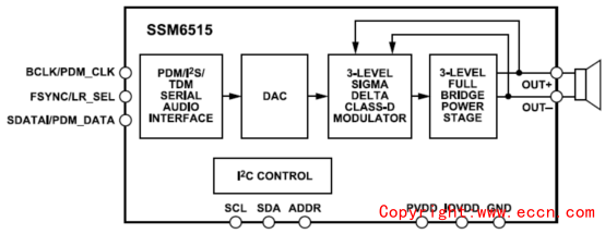
图1. SSM6515功能框图
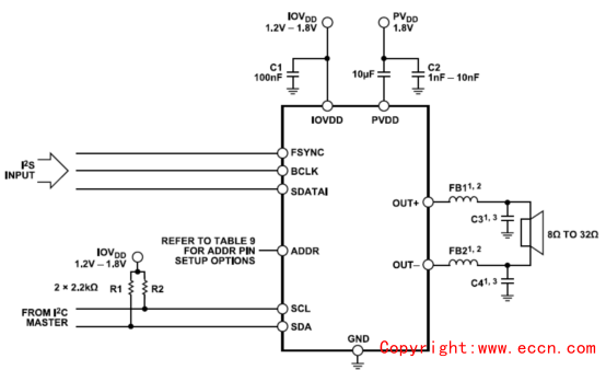
图2. SSM6515典型应用电路图
评估板EVALSSM6515Z
This user guide explains the design and setup of the EVALSSM6515Z evaluation board. The EVAL-SSM6515Z provides access to all analog and digital inputs/outputs on the SSM6515.
The SSM6515 amplifier is controlled by Analog Devices, Inc.,SigmaStudio® software, which interfaces to the EVAL-SSM6515Z via a USB connection. The EVAL-SSM6515Z can be powered by the USB bus or by a single 3.8 V to 5 V supply. These supplies are
regulated to the voltages required on the EVAL-SSM6515Z. The printed circuit board (PCB) is a 4-layer design, with a ground plane and a power plane on the inner layers. The EVAL-SSM6515Z contains 0.1 in. pitch male headers for connecting to external speakers.
The minimum speaker load must be 8 Ω. The EVAL-SSM6515Z consists of two SSM6515s for evaluating the stereo headphone output.
For full details on the SSM6515, see the SSM6515 data sheet, which must be consulted in conjunction with this user guide when using the EVAL-SSM6515Z.
评估板EVALSSM6515Z 包含:
► EVAL-SSM6515Z evaluation board
► EVAL-ADUSB2EBZ (USBi) communications adapter
► USB cable with mini USB plug
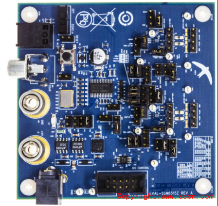
图3. 评估板EVALSSM6515Z外形图
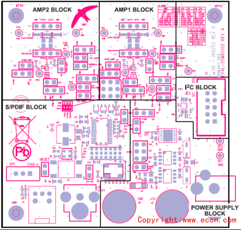
图4. 评估板EVALSSM6515Z框图
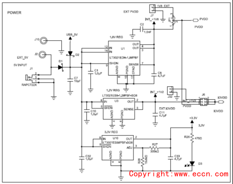
图5. 评估板EVALSSM6515Z电路图
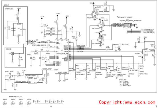
图6. 评估板EVALSSM6515Z电路图(1)
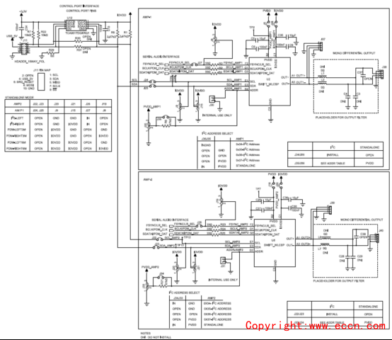
图7. 评估板EVALSSM6515Z电路图(2)
材料清单:
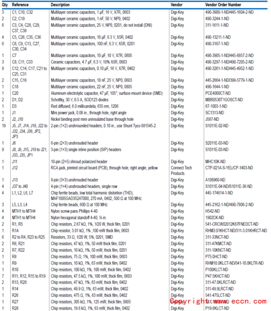
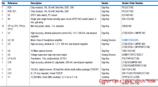
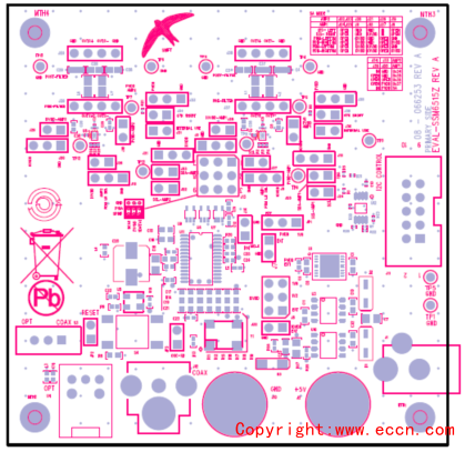
图8. 评估板EVALSSM6515Z PCB设计图:顶层装配
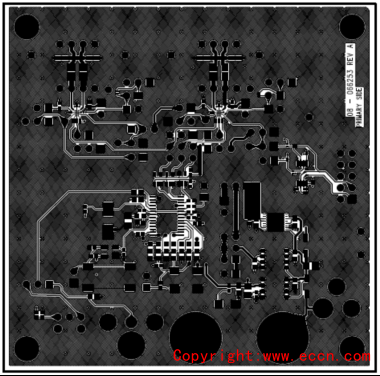
图9. 评估板EVALSSM6515Z PCB设计图:顶层铜
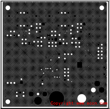
图10. 评估板EVALSSM6515Z PCB设计图:地平面
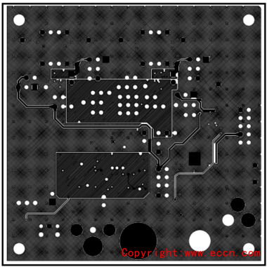
图11. 评估板EVALSSM6515Z PCB设计图:电源平面
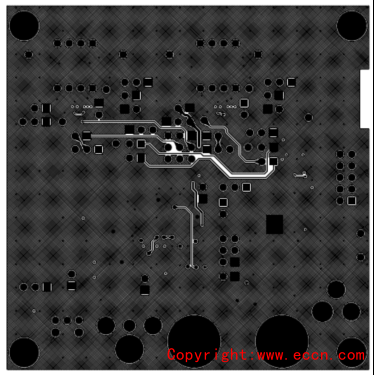
图12. 评估板EVALSSM6515Z PCB设计图:底层铜
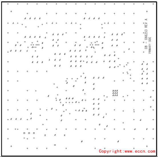
图13. 评估板EVALSSM6515Z PCB设计图:制造图
|

