|
ADI公司的LTC7818是一款高性能三路输出(降压/降压/升压)同步DC/DC开关稳压器控制器,可驱动全部N通道功率MOSFET级,可在4.5 V至40V的宽输入电源电压范围内工作,其恒频电流模式架构允许高达3 MHz的锁相开关频率.极低的空载静态电流可延长电池供电系统的工作运行时间,通过OPTI-LOOP补偿功能,可在宽输出电容和ESR值范围内优化瞬态响应.LTC7818具有一个用于降压的精确0.8V基准电压源,一个用于升压的1.2V基准电压源,和一个电源正常输出指示器.它还具有扩频运行模式,可显著降低输入和输出电源的峰值辐射和传导噪声,能够轻松满足电磁干扰(EMI)标准要求.主要应用在汽车和运输,工业和军事/航空电子.本文介绍了LTC7818主要特性,功能框图和多种应用电路,以及演示板DC2855A主要特性和指标,电路图,材料清单和PCB设计图.
The LTC.7818 is a high performance triple output (buck/buck/boost) synchronous DC/DC switching regulator controllerthat drives all N-channel power MOSFET stages.
Its constant-frequency current mode architecture allowsa phase-lockable switching frequency of up to 3MHz.The LTC7818 operates from a wide 4.5V to 40V inputsupply range. When biased from the output of the boostconverter or another auxiliary supply, the LTC7818 canoperate from an input supply as low as 1V after start-up.
The LTC7818 synchronous boost PassThru capabilityminimizes losses in automotive start-stop applications.The very low no-load quiescent current extends operatingrun time in battery powered systems. OPTI-LOOP.Compensationallows the transient response to be optimizedover a wide range of output capacitance and ESR values.
The LTC7818 features a precision 0.8V reference for thebucks, 1.2V reference for the boost and a power goodoutput indicator.
The LTC7818 additionally features spread spectrum operationwhich significantly reduces the peak radiated andconducted noise on both the input and output supplies,making it easier to comply with electromagnetic interference(EMI) standard
LTC7818主要特性:
nDual Buck Plus Single Boost Synchronous Controllers
nLow Operating IQ:
n14μA (14V to 3.3V, Channel 1 On)
nOutputs Remain in Regulation Through Cold CrankDown to 1V Input Supply Voltage
nWide Bias Input Voltage Range: 4.5V to 40V
nBuck and Boost Output Voltages Up to 40V
nSpread Spectrum Operation
nRSENSE or DCR Current Sensing
nProgrammable Fixed Frequency (100kHz to 3MHz)
nPassThru™/100% Duty Cycle Capable forSynchronous Boost MOSFET
nPhase-Lockable Frequency (100kHz to 3MHz)
nSelectable Continuous, Pulse-Skipping, or LowRipple Burst Mode Operation at Light Loads
nBoost Channel Current Monitor Output
nLow Shutdown IQ: 1.5μA
nSmall 40-Lead 6mm × 6mm QFN Package
nAEC-Q100 Qualified for Automotive Applications
LTC7818应用:
nAutomotive and Transportation
nIndustrial
nMilitary/Avionics
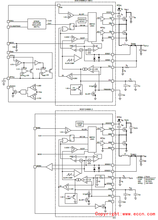
图1.LTC7818功能框图
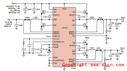
图2. LTC7818典型应用电路图(1)
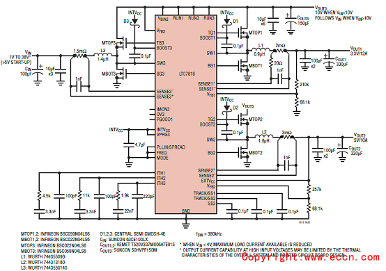
图3. LTC7818典型应用电路图(2)
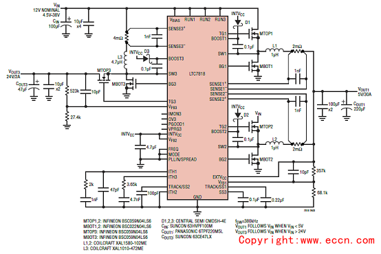
图4. LTC7818典型应用电路图(3)
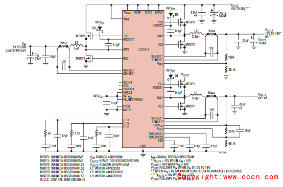
图5. LTC7818典型应用电路图(4)
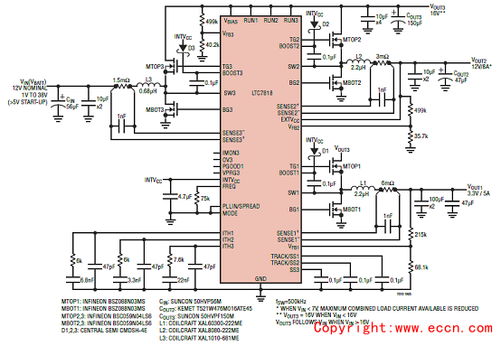
图6. LTC7818典型应用电路图(5)
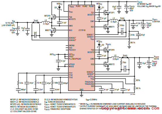
图7. LTC7818典型应用电路图(6)
演示板DC2855A
Demonstration circuit DC2855A is a triple output synchronousstep-up/dual step-down supply featuring theLTC®7818. The demonstration circuit is designed for twobuck outputs 5V/10A, 3.3V/10A supplied by a boosted10V output. Benefiting from this feature, the buck outputsare able to maintain regulation over a wide input voltagerange of 4.5V to 36V which is suitable for automotive orother battery fed applications. Also, the demonstrationcircuit uses a drop-in layout whereas the main buck circuitcomponents fit in an area of .” by 1½”, while the mainboost circuit area is .” by 1.”. The package style for theLTC7818 is a 40-pin exposed pad QFN.
All registered trademarks and trademarks are the property of their respective owners.
演示板DC2855A主要特性:
The main features of the board include rail tracking (Buckchannels only), an internal 5V linear regulator for bias,separated RUN pins for each output, a PGOOD signal(CH1 only), an overvoltage indicator for CH3 and a Modeselector that allow the converter to run in CCM, Pulseskippingor Burst Mode operation. Spread SpectrumMode is availiable for EMI improvement. Synchronizationto an external clock is also possible. The LTC7818 datasheetgives a complete description of these parts, operationand application information. The datasheet must beread in conjunction with this quick start guide for democircuit 2855A.
演示板DC2855A主要指标:
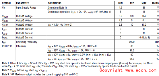
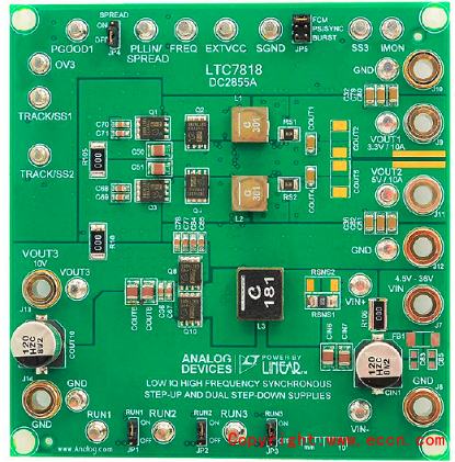
图8.演示板DC2855A外形图
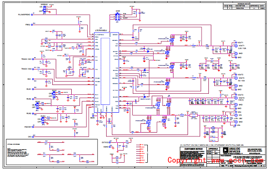
图9.演示板DC2855A电路图(1)
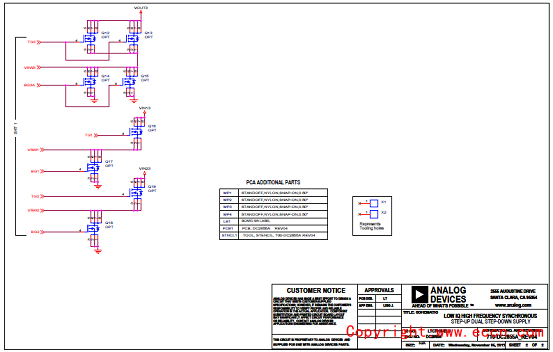
图10.演示板DC2855A电路图(2)
演示板DC2855A材料清单:

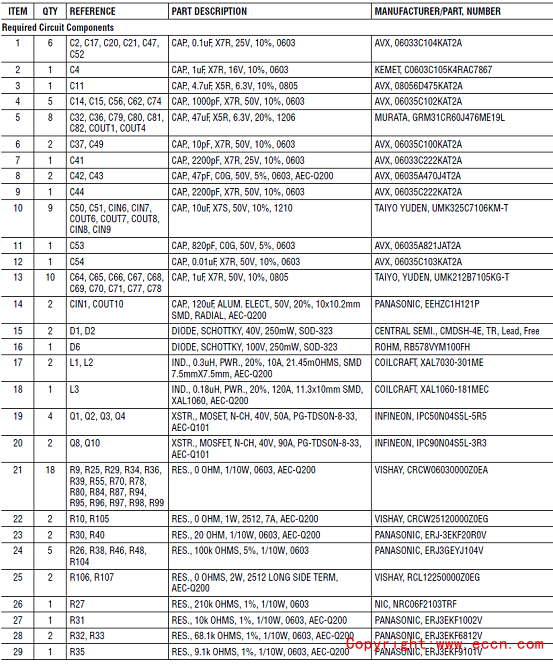
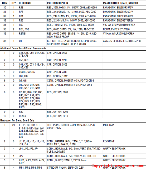
图11.演示板DC2855A PCB设计图(1)
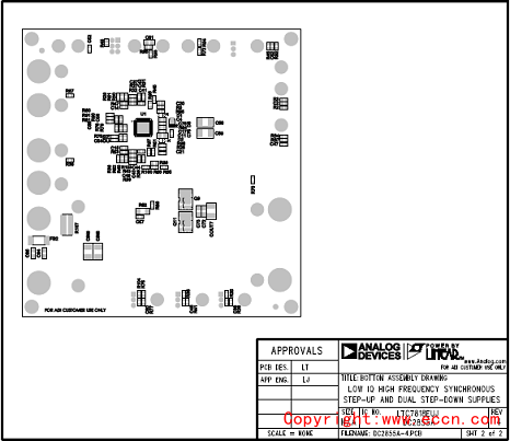
图12.演示板DC2855A PCB设计图(2)
|