 |
|
| |
|
|
ҵ��Ǣ̸��
��ϵ�ˣ���˳ƽ
�ֻ���17727550196����ͬ�ţ�
QQ:3003262363
EMAIL:zsp2018@szczkjgs.com
��ϵ�ˣ�۳�Ȼ�
�ֻ���17727552449 ����ͬ�ţ�
QQ:2850985542
EMAIL:yanxianhui@szczkjgs.com
���������緽ʽ��
�ֻ���13713728695����ͬ�ţ�
QQ:3003207580
EMAIL:panbo@szczkjgs.com
��ϵ�ˣ��˲� |
|
|
| |
|
 |
|
 |
��ǰλ�ã���ҳ -> ������� |
|
|
| TPS63802��Ч2A�������ѹ����ѹת����������� |
|
|
| ������Դ���������Ƽ� ����ʱ�䣺2019/10/19 10:28:00 |
|
TI��˾��TPS63802��Ч�������ѹ-��ѹת����,�������ѹ�ɸ���,���ڻ���������ѹ.��������ںܿ���ѹ��Χ�ڸߴ�2A.��������ѹģʽ��ֵ������4.5A,�ڽ�ѹģʽΪ3.5A,�����ѹ�ɱ�̵���.�ܸ��������ѹ�Զ��ӽ�ѹ�任����ѹģʽ,�������ѹ��Լ���������ѹʱ����ά��3�����ڵĽ�ѹ-��ѹģʽ.�����ѹ��Χ1.3V-5.5V,�����ѹ��Χ1.8V-5V(�ɵ���).��Ҫ����ϵͳԤ��ѹ(�����ֻ�,ƽ�����,EFT�ն˺�Զ��ͨ��ϵͳ),�㸺����ѹ(���ߴ�����,�˿�/�����������ͼ��ܹ�),ָ��,�沿ID,�����������(�����ֻ�,����������,IP���������),RF�Ŵ�����Դ(���ܴ�����),�ȵ��豸(TCE/TEM)��Դ(����ͨ��,��ģ��,����/����).���Ľ�����TPS63802��Ҫ����,���ܿ�ͼ��Ӧ�õ�·,�Լ�����ģ��TPS63802EVM��Ҫ����,��·ͼ,�����嵥��PCB���ͼ.
The TPS63802 is a high efficiency, high outputcurrent buck-boost converter. It is used when theinput voltage is higher, equal, or lower than the outputvoltage. Output currents up to 2 A are supported overa wide voltage range. The device limits the peakcurrent at 4.5 A in Boost-Mode and 3.5 A in Buck-Mode. The device is adjusted to the programmed output voltage. It automatically changes from buck toboost operation based on the input voltage. Itremains in a 3-cycle buck-boost mode when the inputvoltage is approximately equal to the output voltage.
The transitions happen seamlessly and avoidsunwanted toggling within the modes. The TPS63802comes in a 2 mm x 3 mm package. The device workswith tiny passive components to keep the overallsolution size small.
TPS63802��Ҫ����:
1• Input Voltage Range: 1.3 V to 5.5 V
�C >1.8 V for Device Start-up
• Output Voltage Range: 1.8 V to 5 V (adjustable)
• 2-A Output Current for VIN �� 2.3 V, VOUT = 3.3 V
• High Efficiency Over the Entire Load Range
�C Power Save Mode with Mode Selection
• Peak Current Buck-Boost Mode Architecture
�C Seamless Transition Between Buck, Buck-Boost and Boost operation modes
�C Operates With Low and High OutputCapacitance values
�C Forward and Reverse Current Operation
�C Start-up Into Pre-Biased Outputs
• Safety- and Robust Operation Features
�C Integrated Soft Start
�C Over-Temperature- and Over-Voltage-Protection
�C True Shutdown Function with Load Disconnect
�C Forward and Backward current limit
• Small Solution Size
�C 2 mm x 3 mm Package size
�C Small 0.47 ��H inductor
�C Works With 22��F Minimum Output Capacitor
• Create a Custom Design Using the TPS63802With the WEBENCH® Power Designer
TPS63802Ӧ��:
• System Pre-Regulator (Smartphone, Tablet, EFTTerminal, Telematics)
• Point-of-Load Regulation (Wired Sensor,Port/Cable Adapter and Dongle)
• Fingerprint, Face-ID, Camera Sensors(Smartphone, Electronic Smart Lock, IP Network Camera)
• RF Amplifier Supply (Smart Sensors)
• Thermoelectric Device (TEC/TEM) Supply(Datacom, Optical Modules, Cooling/Heating)
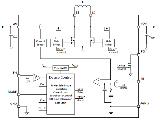
ͼ1.TPS63802���ܿ�ͼ
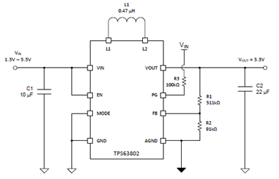
ͼ2.TPS63802 3.3VoutӦ�õ�·ͼ
����ģ��TPS63802EVM
This user��s guide describes the operation, and use of the TPS63802EVM evaluation module (EVM). TheTPS63802EVM is designed to help the users easily evaluate and test the operation and functionality of theTPS63802 buck-boost converter. The TPS63802EVM has the output voltage set to 3.3 V. The EVMoperates from 1.3 V to 5.5 V input voltage. Output current can go up to 2 A in buck mode and boost mode.
This document includes setup instructions for the hardware, a schematic diagram, a bill of materials(BOM), and printed-circuit board (PCB) layout drawings for the evaluation module. Throughout thisdocument, the abbreviations EVM, TPS63802EVM, and the term evaluation module are synonymous withthe TPS63802, unless otherwise noted.
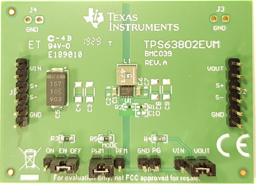
ͼ3.����ģ��TPS63802EVM����ͼ
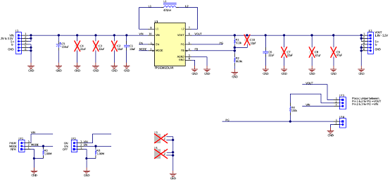
ͼ4.����ģ��TPS63802EVM��·ͼ
����ģ��TPS63802EVM�����嵥:

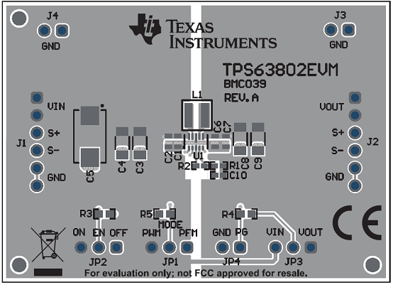
ͼ5.����ģ��TPS63802EVM PCBװ��ͼ
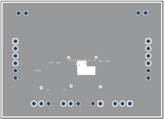
ͼ6.����ģ��TPS63802EVM PCB�źŲ�1
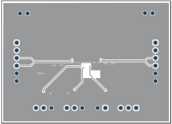
ͼ7.����ģ��TPS63802EVM PCB�źŲ�2
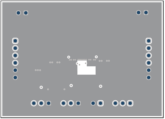
ͼ8.����ģ��TPS63802EVM PCB�ײ�����ͼ
|
|
| |
| |
|
|
|

