 |
|
| |
|
|
ҵ��Ǣ̸��
��ϵ�ˣ���˳ƽ
�ֻ���17727550196����ͬ�ţ�
QQ:3003262363
EMAIL:zsp2018@szczkjgs.com
��ϵ�ˣ�۳�Ȼ�
�ֻ���17727552449 ����ͬ�ţ�
QQ:2850985542
EMAIL:yanxianhui@szczkjgs.com
���������緽ʽ��
�ֻ���13713728695����ͬ�ţ�
QQ:3003207580
EMAIL:panbo@szczkjgs.com
��ϵ�ˣ��˲� |
|
|
| |
|
 |
|
 |
��ǰλ�ã���ҳ -> ������� |
|
|
| L9907����BLDC��������������� |
|
|
| ������Դ���������Ƽ� ����ʱ�䣺2019/4/16 9:58:00 |
|
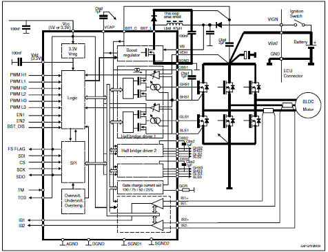
ST��˾��L9907������դ��������,����ST��˾���Ƚ���BCD-6s����,����������3��BLDC���������PowerMOS�����L9907���������淶AEC-Q100,��Դ��ѹ��4.2V��54V,���ڹ����ڵ�(12V)ϵͳ,˫(24V)ϵͳ��48V���Ӧ��,��FET�߱��������������ܾ���ס-7 V - 90 V,�ʹ�����������,PWM����Ƶ�ʸߴ�20kHz,դ��������������ͨ��SPI�IJ�����,������Χͨ����ӵ������դ�����Ƶ���Ϊ600mA.����б�������Ϲ���:FET���������е�ԴǷѹ(UV)���,դ��Դ�����ѹ����,դ��Դ��Դ���ضϿ�;��ԴVB��VCC�й�ѹ(OV),Ƿѹ(UV)��Ϻͱ�������,�����������ܾ���35V,������Ϻض�,��Ҫ����3��դ��������������FET������.���Ľ�����L9907��Ҫ����,��ͼ,�����������ͼ�Լ�������EVAL-L9907Ӧ�ÿ�ͼ,�����·ͼ����������·ͼ����PCB���ͼ.
L9907 is a smart power device realized in STMicroelectronics advanced BCD-6s technology. It is able to drive all PowerMOS transistors for 3-phase BLDC motor applications. The circuit is suitable to operate in environments with high supply voltage such as double battery. Supply related pins are capable of withstanding up to 90 V. Moreover, the device is able to control the six pre-driver channels independently. In this way it is possible to implement all kinds of electric motor control strategy.
The integrated boost regulator provides sufficient gate charge for all PowerMOS down to a battery voltage of 6 V. All pre-drivers have dedicated connections with the MOSFET sources. The device offers programmability for a base gate output current via an external resistor. Moreover, via SPI, it is possible to select among 4 gate output current levels even while the application is running. All channels are protected against short circuit and the device is protected against overtemperature conditions. Moreover, the boost converter implements an over voltage protection to allow safe functionality of pre-drivers in all battery voltage conditions. During over voltage conditions, BST_C voltage is limited by temporarily switching off the boost regulator and pre-drivers are allowed to operate. Boost will be self re-enabled as soon as the output voltage decreases to an acceptable value.
The device is equipped with 2 current sense amplifiers. Both have SPI selectable amplifier gain (10, 30, 50 and 100) and output offset voltage level in order to allow max flexibility for phase or ground current sense strategy. All I/O pins are 35 V compatible. Full diagnostic is available through SPI. The device is available in TQFP64 and bare die, depending on the application requirements.The device is protected against Shoot Through events.
L9907��Ҫ����:
AEC-Q100 qualified
Supply voltage from 4.2V to 54 V for working in single (12 V systems), double (24 V systems) and 48 V battery applications
The device can withstand -7 V to 90 V at the FET high-side Driver pins
Low standby current consumption
3.3 V internal regulator supplied by Vcc pin
Boost regulator for full Rdson down to 6 V and over voltage protection
3 low-side + 3 high-side drivers
�C PWM operation up to 20 kHz
�C Gate driver current adjustable via SPI in 4 steps. Range set via external resistor. Maximum gate controlled current 600 mA
�C Source connection to each MOSFET
Input pin for each gate driver
2-differential current sense amplifiers:
�C Output offset selectable via SPI (0.2*Vcc offset for ground shunt resistors connection, 0.5*Vcc offset for phase shunt resistors connection)
�C All the amplifier gain factors are programmable (10, 30, 50, 100)
8 MHz, 16-bit SPI
Full diagnostic
Programmable parameters:
�C Cross conduction dead time with a fixed minimum value
�C 4 current steps driving the PowerMOS gates (25%, 50%, 75%, 100%)
�C Phase or ground selection of current sense amplifier
�C Gain values for the current sense amplifiers
�C Zero current output voltage (offset) for the current sense amplifiers
�C Over voltage threshold selection for single or double battery operation
�C Short circuit detection thresholds for the low-side and the high-side MOSFETs (drain to source voltage monitor).
Protection and diagnostic
FET driver:
�C FET driver supply Undervoltage (UV) diagnostic;
�C Gate to source output voltage limit;
�C Gate to source passive switch off.
Power supply pins VB and VCC:
�C Overvoltage (OV), Undervoltage (UV) diagnostic and protection
All logic pins withstand 35 V
Power MOSFET drain to source voltage drop measurement for overcurrent protection Over-temperature diagnostic and shutdown
Fault status flag output
ͼ1.L9907��ͼ
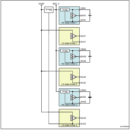
ͼ2.MOSFET��������Դ�ܹ�ͼ
ͼ3.�����������ͼ
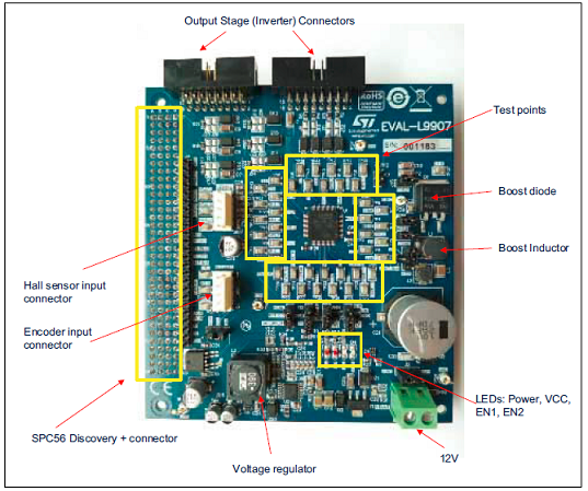
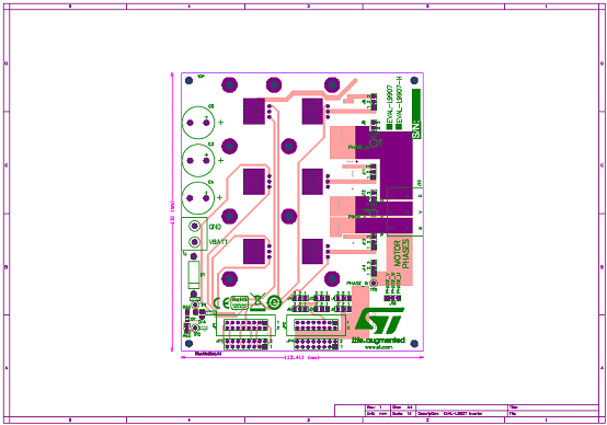
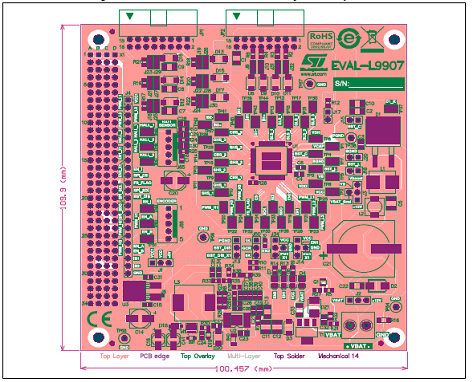
������EVAL-L9907
The EVAL-L9907 is an evaluation board designed to provide the user a platform for the L9907, a FET driver for 3 phase BLDC motor. The board offers all the main input/output capabilities needed to drive a BLCD motor properly and to provide diagnostic functionalities.
Full diagnostic is available through SPI. By using SPI communication, it is possible to program L9907 while the application is running (e.i. set the gain of the current sense amplifier).
A dedicated pin array allows connecting easily a SPC5 discovery+ board and the EVAL-L9907. In association with the discovery board SPC560P-DISP a dedicated SW allows controlling a motor control application by using a PC via a USB port.
L9907 device is able to control the six pre-driver channels independently and all pre-drivers have dedicated connections with the output MOSFETs; this feature gives the user the possibility to implement all kinds of electric motor control strategy. All gate driver outputs are protected against short circuit and L9907 is protected against over-temperature condition.
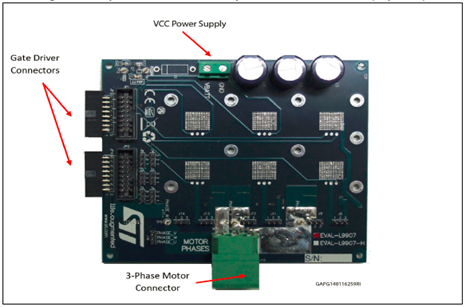
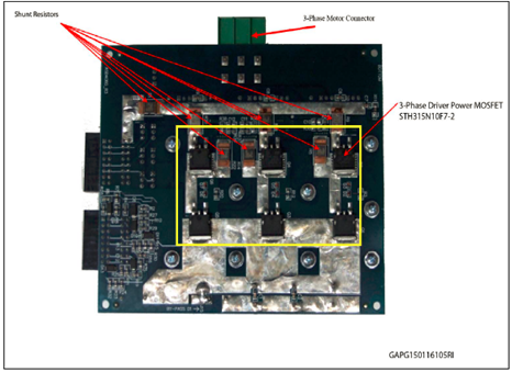
Three terminal blocks are dedicated to connect the three wires of a BLDC Motor (3-phases), moreover, specific connectors are present to connect the feedback signals from the motor to the gate driver and to the microcontroller.
The EVAL-L9907 is an evaluation board designed to allow the whole hardware configuration flexibility, giving the user total access to all pins of the L9907.
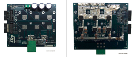
Standard connectors connect the gate driver board (L9907) and Inverter Power MOSFET output stage; this solution allows simplifying the evaluation procedure and it increases the flexibility of the HW environment.
The main features are: Total accessibility to all device pins (both L9907 and the Inverter MOSFET board).Two separated boards: gate driver with L9007 and Inverter Power MOSFET boards with the MOSFET array. This HW architecture allows the user to evaluate the application with different HW configurations. Output power board current capability up to 20A.Full HW compatibility with the SPC56 discovery boards through the standard SPC56 Discovery+ connector, 0.1�� - 4x36 pin.Possibility to connect generic microcontroller boards(a) by using a customized adapter.
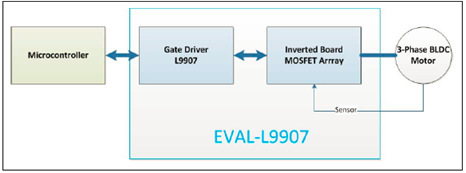
ͼ4.������EVAL-L9907Ӧ�ÿ�ͼ
ͼ5.L9907դ����������-Ԫ����������-����

ͼ6.L9907դ����������-Ԫ����������-�ײ�
ͼ7.L9907�����Դ������ͼ-����ͼ8.L9907�����Դ������ͼ-�ײ�
ͼ9.L9907�����Դ��-Ԫ����������-����
ͼ10.L9907�����Դ��-Ԫ����������-�ײ�
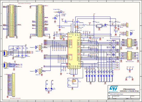
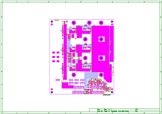
ͼ11.������EVAL-L9907�����·ͼ(1)
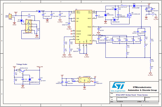
ͼ12.������EVAL-L9907�����·ͼ(2)
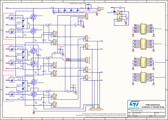
ͼ13.������EVAL-L9907��������·ͼ
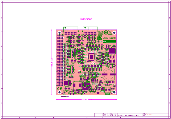
ͼ14.������EVAL-L9907����PCB���ͼ(1)
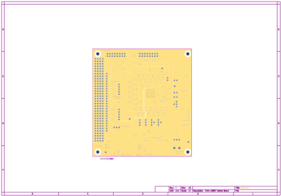
ͼ15.������EVAL-L9907����PCB���ͼ(2)
ͼ16.������EVAL-L9907����PCB���ͼ(3)
ͼ17.������EVAL-L9907����PCB���ͼ(4)
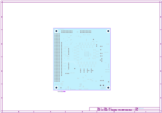
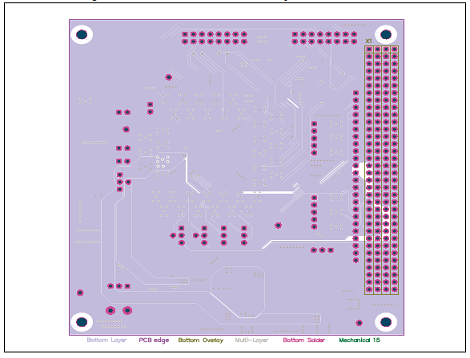
ͼ18.������EVAL-L9907�������PCB���ͼ(1)
ͼ19.������EVAL-L9907�������PCB���ͼ(2)

ͼ20.������EVAL-L9907�������PCB���ͼ(3)
ͼ21.������EVAL-L9907�������PCB���ͼ(4)
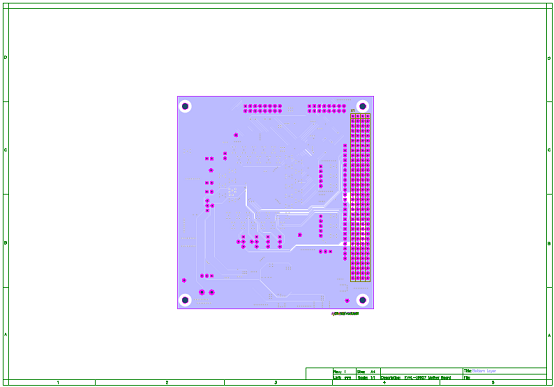
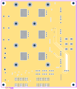
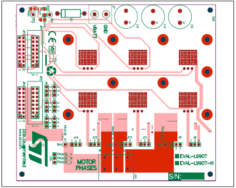
ͼ22.������EVAL-L9907դ����������PCB����ͼ-����
ͼ23.������EVAL-L9907դ����������PCB����ͼ-�ײ�
ͼ24.������EVAL-L9907�������PCB����ͼ-����
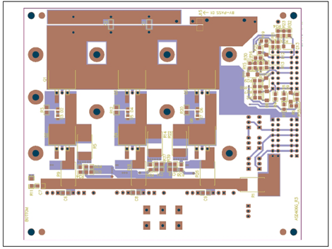
ͼ25.������EVAL-L9907դ����������PCB����ͼ-�ײ�
|
|
| |
| |
|
|
|