 |
|
| |
|
|
业务洽谈:
联系人:张顺平
手机:17727550196(微信同号)
QQ:3003262363
EMAIL:zsp2018@szczkjgs.com
联系人:鄢先辉
手机:17727552449 (微信同号)
QQ:2850985542
EMAIL:yanxianhui@szczkjgs.com
负责人联络方式:
手机:13713728695(微信同号)
QQ:3003207580
EMAIL:panbo@szczkjgs.com
联系人:潘波 |
|
|
| |
|
 |
|
 |
当前位置:首页 -> 方案设计 |
|
|
| NXP Kinetis KV111KW D类音频放大器参考设计 |
|
|
| 文章来源: 更新时间:2016/6/12 14:54:00 |
|
NXP公司的Kinetis KV10和KV11采用ARM Cortex-M0+内核和蔼创新的90nm薄膜存储器(TFS)闪存技术,工作频率高达75MHz,多达128KB程序闪存,多达16KB RAM,工作电压1.71到3.6 V,主要用在工业马达控制,逆变器和低端电源转换应用.本文介绍了Kinetis KV1x MCU主要特性,框图和1000W D类音频放大器参考设计主要特性,电路图和PCB元件布局图.
The Kinetis V Series KV11x MCU family is built on ARM Cortex-M0+ core and enabled by innovative 90nm thin film storage(TFS) flash process technology. The KV11x is an extension ofthe existing KV10x family providing increased memory, higherpin count, additional FTMs and a FlexCAN serial interface.
KV11x is ideal for industrial motor control applications, inverters,and low-end power conversion applications.
Kinetis KV1x MCU主要特性:
Performance
• Up to 75 MHz ARM Cortex-M0+ based core
Memories and memory interfaces
• Up to 128 KB of program flash memory
• Up to 16 KB of RAM
System peripherals
• Nine low-power modes to provide power optimizationbased on application requirements
• 8-channel DMA controller
• SWD interface and Micro Trace buffer
• Bit Manipulation Engine (BME)
• External watchdog timer
• Advanced independent clocked watchdog
• Memory Mapped Divide and Square Root (MMDVSQ)module
Clocks
• 32-40 kHz or 4-32 MHz external crystal oscillator
• Multipurpose clock generator (MCG) with frequencylockedloop referencing either internal or externalreference clock
Security and integrity modules
• 80-bit unique identification (ID) number per chip
• Hardware CRC module
Communication interfaces
• One 16-bit SPI module
• One I2C module
• Two UART modules
• One FlexCAN module1
Timers
• Programmable delay block
• Two 6-channelFlexTimers (FTM) for motor control/general purpose applications
• Four 2-channelFlexTimers (FTM) with quadraturedecoder functionality
• 16-bit low-power timer (LPTMR)
Operating Characteristics
• Voltage range: 1.71 to 3.6 V
• Flash write voltage range: 1.71 to 3.6 V
• Temperature range (ambient): –40 to 105℃
Analog modules
• Two 16-bit SAR ADCs
• 12-bit DAC
• Two analog comparators (ACMP) containing a 6-bitDAC and programmable reference input
Human-machine interface
• General-purpose I/O
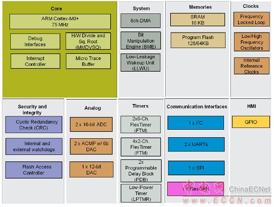
图1.Kinetis KV1x MCU框图
1000W D类音频放大器参考设计
The 1000 W class-D audio amplifier reference design is intended to provide an example for an audio amplifier along with a push-pull power converter and operates using the Kinetis KV1x Tower series platform or k64 Freedom board. This reference design uses the internal powerful FlexTimer module for modulating the input analog audio on a class-D format and for generating the PWM to control the switching push-pull power supply.
1000W D类音频放大器参考设计主要特性:
Prototype quickly using the Tower System module or Freedom System platform to capture analogical audio input, generate the class-D audio output and to control the push-pull power supply.
Together with embedded source code, quickly build an affordable class-D audio amplifier.
Flextimer controls the gate drivers for power Mosfets adding extra protections, such as deadtime insertion, fault control, initialization and polarity control.
Low CPU load, leaving processor available application enhancement.
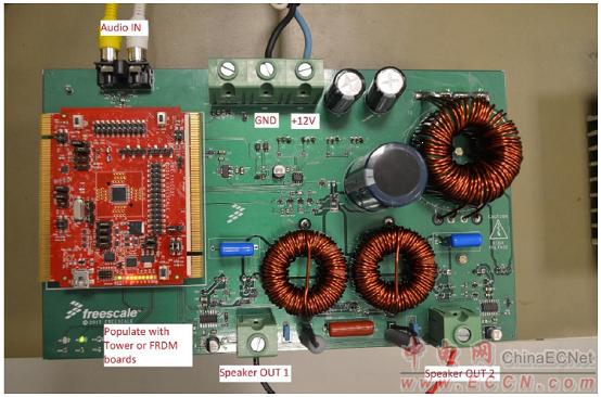
图2.1000W D类音频放大器参考设计外形图
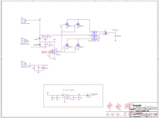
图3.1000W D类音频放大器参考设计电路图(1)
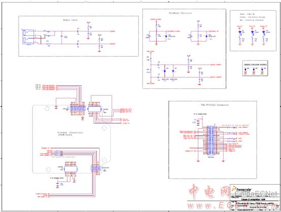
图4.1000W D类音频放大器参考设计电路图(2)
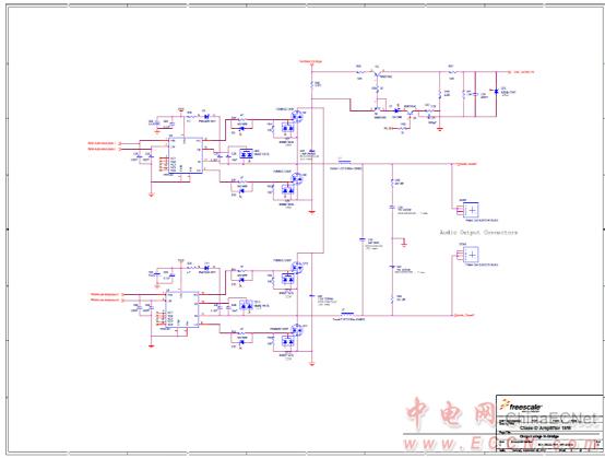
图5.1000W D类音频放大器参考设计电路图(3)
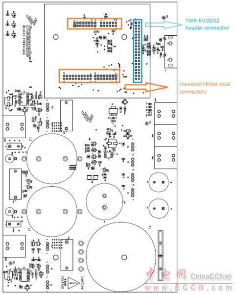
图6.1000W D类音频放大器参考设计PCB元件分布图
|
|
| |
| |
|
|
|

