 |
|
| |
|
|
Ò”ÎńÇąÌžŁș
ÁȘÏ”ÈËŁșŐĆËłÆœ
ÊÖ»úŁș17727550196ŁšÎąĐĆÍŹșĆŁ©
QQ:3003262363
EMAIL:zsp2018@szczkjgs.com
ÁȘÏ”ÈËŁșÛłÏÈ»Ô
ÊÖ»úŁș17727552449 ŁšÎąĐĆÍŹșĆŁ©
QQ:2850985542
EMAIL:yanxianhui@szczkjgs.com
žșÔđÈËÁȘÂ緜ʜŁș
ÊÖ»úŁș13713728695ŁšÎąĐĆÍŹșĆŁ©
QQ:3003207580
EMAIL:panbo@szczkjgs.com
ÁȘÏ”ÈËŁșĆËČš |
|
|
| |
|
 |
|
 |
”±Ç°Î»ÖĂŁșÊŚÒł -> ·œ°žÉèŒÆ |
|
|
| AD5676”ÍčŠșÄ8Íš”À16λDACœâŸö·œ°ž |
|
|
| ÎÄŐÂÀŽÔŽŁș žüĐÂʱŒäŁș2015/5/15 9:28:00 |
|
ADIč«ËŸ”ÄAD5676RÊÇ”ÍčŠșÄ8Íš”À16λ»șłć”çŃčÊäłöÊęÄŁŚȘ»»Æś(DAC),ÄÚÖĂ2.5V 2 ppm/˚CÄÚČż»ùŚŒ”çŃčÔŽșÍÉϔ瞎λ”ç·,ČÉÓöàčŠÄÜŽźĐĐÍâÉèœÓżÚ(SPI)ŁŹÊ±ÖÓËÙÂÊŚîžßŽï50 MHz, 而śÎ¶È−40Ąæ ”œ+125Ąæ,而ś”çŃč2.7 V”œ5.5 V,ÖśÒȘÓĂÔÚčâÊŐ·ąÆś,»ùŐŸčŠÂÊ·ĆŽóÆś,čęłÌżŰÖÆŁšżÉ±àłÌÂߌżŰÖÆ[PLC]I/OżšŁ©,č€Ò”ŚÔ¶Ż»ŻșÍÊęŸĘČÉŒŻÏ”Íł.±ŸÎÄœéÉÜÁËAD5672R/AD5676RÖśÒȘÌŰĐÔ,čŠÄÜżòÍŒ,ŸŐ»šÁŽœÓÍŒÒÔŒ°AD5676RÆÀčÀ°ćÖśÒȘÌŰĐÔ,żòÍŒ,”ç·͌șÍČÄÁÏÇ攄.
The AD5672R/AD5676R are low power, octal, 12-/16-bit buffered voltage output digital-to-analog converters (DACs). They include a 2.5 V, 2 ppm/Ąæ internal reference (enabled by default) and a gain select pin giving a full-scale output of 2.5 V (gain = 1) or 5 V (gain = 2). The devices operate from a single 2.7 V to 5.5 V supply and are guaranteed monotonic by design. The AD5672R/AD5676R are available in a 20-lead TSSOP package and incorporate a power-on reset circuit and a RSTSEL pin that ensures that the DAC outputs power up to zero scale or midscale and remain there until a valid write. The AD5672R/AD5676R contain a power-down mode, reducing the current consumption to 1 ŠÌA typical while in power-down mode.
AD5672R/AD5676RÖśÒȘÌŰĐÔ:
High performance
High relative accuracy (INL): ĄÀ3 LSB maximum at 16 bits
Total unadjusted error (TUE): ĄÀ0.14% of FSR maximum
Offset error: ĄÀ1.5 mV maximum
Gain error: ĄÀ0.06% of FSR maximum
Low drift 2.5 V reference: 2 ppm/Ąæ typical
Wide operating ranges
−40Ąæ to +125Ąæ temperature range
2.7 V to 5.5 V power supply
Easy implementation
User selectable gain of 1 or 2 (GAIN pin)
1.8 V logic compatibility
50 MHz SPI with readback or daisy chain
Robust 2 kV HBM and 1.5 kV FICDM ESD rating
20-lead, TSSOP RoHS-compliant package
AD5672R/AD5676RÓŠÓĂ:
Optical transceivers
Base station power amplifiers
Process control (PLC input/output cards)
Industrial automation
Data acquisition systems
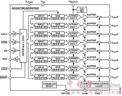
ÍŒ1. AD5672R/AD5676RčŠÄÜżòÍŒ
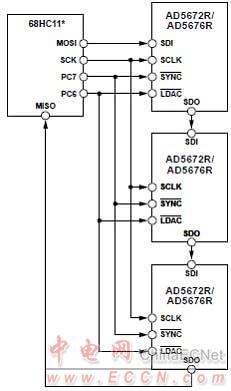
ÍŒ2. AD5672R/AD5676RŸŐ»šÁŽœÓÍŒ
AD5676RÆÀčÀ°ćEVAL-AD5676SDZ/EVAL-AD5676RSDZ
This user guide details the operation of the evaluation boards for the AD5676/AD5676R octal channel, voltage output digital-to-analog converter (DAC).
The EVAL-AD5676SDZ/EVAL-AD5676RSDZ evaluation boards help users to quickly prototype new AD5676/AD5676R circuits and reduce design time. The AD5676/AD5676R operate from a single 2.7 V to 5.5 V supply. The AD5676R has an internal 2.5 V reference giving a maximum output voltage of 2.5 V or 5 V. The AD5676 does not have an internal reference; therefore, an ADR431 is provided on-board as a 2.5 V reference source. A different reference voltage can be applied via the EXT_REF SMB connector, if required. Full data on the AD5676/AD5676R are available in the respective product data sheets, available from Analog Devices, which should be consulted in conjunction with this user guide when using the evaluation boards.
The evaluation boards interface to the USB port of a PC via the SDP board. Software is supplied with the evaluation board to allow the user to program the AD5676/AD5676R.
The evaluation boards are compatible with the EVAL-SDP-CB1Z Blackfin® SDP controller board (SDP-B), which is available for order on the Analog Devices website at www.analog.com.
ÆÀčÀ°ćEVAL-AD5676SDZ/EVAL-AD5676RSDZÖśÒȘÌŰĐÔ:
Full featured evaluation board for the AD5676/AD5676R
Various link options
PC control in conjunction with the Analog Devices, Inc., EVAL-SDP-CB1Z system demonstration platform (SDP)
ÆÀčÀ°ćEVAL-AD5676SDZ/EVAL-AD5676RSDZ°üÀš:
EVAL-AD5676SDZ/EVAL-AD5676RSDZ evaluation board
CD includes
Self-installing evaluation software that allows users to control the board and exercise all functions of the device
Electronic version of the EVAL-AD5676SDZ/ EVAL-AD5676RSDZ user guide
ADDITIONAL EQUIPMENT AND SOFTWARE NEEDED
EVAL-SDP-CB1Z SDP board, includes a USB cable
PC running Windows XP SP2, Windows Vista, or Windows 7 with USB 2.0 port
ONLINE RESOURCES
Documents Needed
AD5676/AD5676R data sheet
EVAL-AD5676SDZ/EVAL-AD5676RSDZ user guide
Required Software
AD5676(R) evaluation software (download from the EVAL-AD5676SDZ/EVAL-AD5676RSDZ product pages)
Design and Integration Files
Schematics, layout files, bill of materials
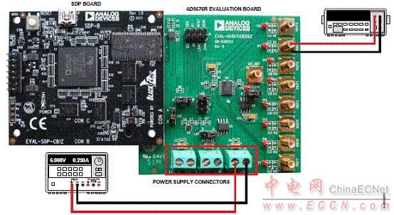
ÍŒ3. ÆÀčÀ°ćEVAL-AD5676SDZ/EVAL-AD5676RSDZœšÁąÍŒ
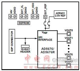
ÍŒ4. ÆÀčÀ°ćEVAL-AD5676SDZ/EVAL-AD5676RSDZżòÍŒ
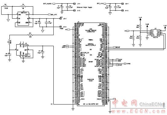
ÍŒ5. ÆÀčÀ°ćEVAL-AD5676SDZ/EVAL-AD5676RSDZ”ç·͌(1)
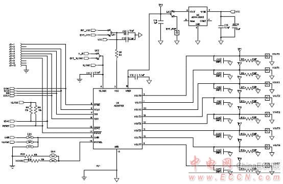
ÍŒ6. ÆÀčÀ°ćEVAL-AD5676SDZ/EVAL-AD5676RSDZ”ç·͌(2)
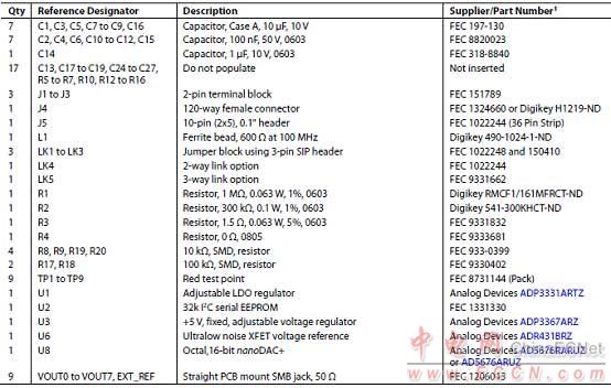
ÆÀčÀ°ćEVAL-AD5676SDZ/EVAL-AD5676RSDZČÄÁÏÇ攄:
AD5672R/AD5676R ·Ö±đÊÇ”ÍčŠșÄĄą8Íš”ÀĄą12/16λ»șłć”çŃčÊäłöÊęÄŁŚȘ»»Æś(DAC)ŁŹÄÚÖĂ2.5 VĄą2 ppm/˚CÄÚČż»ùŚŒ”çŃčÔŽŁšÄŹÈÏÊčÄÜŁ©șÍÔöÒæŃĄÔńÒęœĆŁŹÂúÁżłÌÊäłöÎȘ2.5 VŁšÔöÒæ=1Ł©»ò5 VŁšÔöÒæ=2Ł©ĄŁ ČÉÓĂ2.7 VÖÁ5.5 V”„”çԎ詔磏͚čęÉèŒÆ±ŁÖ€”„”śĐÔĄŁ ŐâĐ©ÆśŒțČÉÓĂ20ÒęœĆTSSOP·âŚ°ĄŁ
AD5672R/AD5676R»čÄÚÖĂÒ»žöÉϔ瞎λ”ç·șÍÒ»žöRSTSELÒęœĆŁŹÈ·±ŁDACÊäłöÉÏ”çÖÁÁă”çÆœ»òÖĐŒä”çÆœŁŹÖ±”œÖŽĐĐÒ»ŽÎÓĐЧ”ÄĐŽČÙŚśÎȘÖ襣 ĂżžöÆśŒț¶ŒŸßÓĐžśÍš”À¶ÀÁą”ô”çÌŰĐÔŁŹÔÚ”ô”çÄŁÊœÏÂŁŹÆśŒțčŠșÄœ”ÖÁ2.5 µAĄŁ
AD5672R/AD5676RČÉÓöàčŠÄÜŽźĐĐÍâÉèœÓżÚ(SPI)ŁŹÊ±ÖÓËÙÂÊŚîžßŽï50 MHzŁŹČąŸù°üșŹÒ»žöÎȘ1.8 V/3 V/5 VÂߌ”çÆœŚŒ±ž”ÄVLOGICÒęœĆĄŁ
ČúÆ·ÌŰÉ«
žßÏà¶ÔŸ«¶È(INL)ĄŁ
AD5672RŁš12λŁ©ŁșĄÀ0.1 LSBŁšŚîŽóÖ”Ł©
AD5676RŁš16λŁ©ŁșĄÀ3 LSBŁšŚîŽóÖ”Ł©
”ÍÆŻÒÆ2.5 VÆŹÄÚ»ùŚŒ”çŃčÔŽĄŁ
|
|
| |
| |
|
|
|

